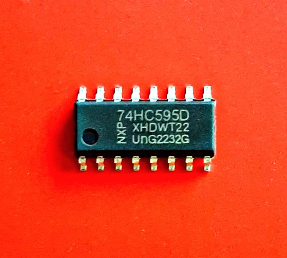


74HC595D SMD 8-bit serial-in IC


Reviews & Ratings
74HC595D SMD 8-bit serial-in IC || 74HC595 NXP SMD IC BUY ONLINE || 74HC595; 74HCT595 8-bit serial-in, serial or parallel-out shift register with output latches; 3-state
The 74HC595; 74HCT595 is an 8-bit serial-in/serial or parallel-out shift register with a storage register and 3-state outputs. Both the shift and storage register have separate clocks. The device features a serial input (DS) and a serial output (Q7S) to enable cascading and an asynchronous reset MR input. A LOW on MR will reset the shift register. Data is shifted on the LOW-to-HIGH transitions of the SHCP input. The data in the shift register is transferred to the storage register on a LOW-to-HIGH transition of the STCP input. If both clocks are connected together, the shift register will always be one clock pulse ahead of the storage register. Data in the storage register appears at the output whenever the output enable input (OE) is LOW. A HIGH on OE causes the outputs to assume a high-impedance OFF-state. Operation of the OE input does not affect the state of the registers. Inputs include clamp diodes. This enables the use of current limiting resistors to interface inputs to voltages in excess of VCC.
Features and benefits :
- Wide supply voltage range from 2.0 to 6.0 V
- CMOS low power dissipation
- High noise immunity
- 8-bit serial input
- 8-bit serial or parallel output
- Storage register with 3-state outputs
- Shift register with direct clear
- 100 MHz (typical) shift out frequency
- Latch-up performance exceeds 100 mA per JESD 78 Class II Level B
Applications :
- Serial-to-parallel data conversion
- Remote control holding register
- Inverter & UPS
74HC595D74HCT595D -40 °C to +125 °C SO16 plastic small outline package; 16 leads; body width 3.9 mm SOT109-1
74HC595D IC Functional diagram :


| Symbol | Pin | Description |
| Q0, Q1, Q2, Q3, Q4, Q5, Q6, Q7 | 15, 1, 2, 3, 4, 5, 6, 7 | parallel data output |
| GND | 8 | ground (0 V) |
| Q7S | 9 | serial data output |
| MR | 10 | master reset (active LOW) |
| SHCP | 11 | shift register clock input |
| STCP | 12 | storage register clock input |
| OE | 13 | output enable input (active LOW |
| DS | 14 | serial data input |
| Q0 | 15 | parallel data output 0 |
| Vcc | 16 | supply voltage |
Frequently Bought Products
Product Queries (0)
Login Or Registerto submit your questions to seller
Other Questions
No none asked to seller yet